By NXP Semiconductors 101

NXP's QN9080SIP is an ultra-small module based on the QN9080 Bluetooth® MCU and NT3H2211 NTAG that delivers industry-leading low-power consumption along with a rich feature set and FCC, CE, IC, and MIC certifications, making it an ideal solution for wearable and battery-powered applications.
Designed to be the perfect enabler for NFC in home automation and consumer applications, this feature-packed, second generation-connected NFC tag is the fastest, least expensive way to add tap-and-go connectivity to just about any electronic device. The QN9080SIP integrates NTAG for out-of-band pairing. By tapping an IoT device based on the QN9080SIP with an NFC reader-embedded device, a Bluetooth low energy connection can be established quickly simplifying the pairing process.
The module is based on the QN9080 Bluetooth MCU powered by an Arm® Cortex®-M4F and integrates a dedicated fusion sensor co-processor (FSP) to further reduce power consumption by offloading complex math computations from the CPU. The 512 kB onboard Flash and 128 kB SRAM provide enough room and flexibility for complex applications and the connectivity stacks.
The module also integrates NFC NTAG, 32 MHz and 32 kHz crystals, RF matching, and a 2.4 GHz antenna and is certified to FCC, CE, IC, and MIC regulations offering a complete and ready-to-use solution for applications requiring Bluetooth low energy wireless connectivity and simple pairing with NFC NTAG. This level of integration reduces overall system size, complexity, and development time.
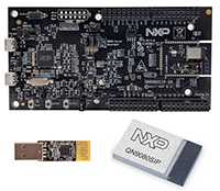
The QN9080SIP DK board is designed to make it as easy as possible to get started with a project based on the QN9080SIP module. Each kit contains one QN9080SIP DK board and one QN9080-based dongle.
The QN9080SIP DK board integrates buttons, a piezo buzzer, and an LED for an easy way to reset the chip and indicate chip status. The DK board also provides useful interfaces such as a USB port for UART communication and CMSIS debug.