CD4056BM96

CD4056BM96
Mfr. #:
CD4056BM96
説明:
LCD Drivers CMOS BCD-to-7-Seg LCD Dec/Driver
ライフサイクル:
メーカー新製品
データシート:
CD4056BM96 データシート
配達:
DHL FedEx Ups TNT EMS
支払い:
T/T Paypal Visa MoneyGram Western Union
ECAD Model:
詳しくは:
CD4056BM96 詳しくは CD4056BM96 Product Details
製品属性
属性値
メーカー:
テキサスインスツルメンツ
製品カテゴリ:
LCDドライバー
JBoss:
Y
シリーズ:
CD4056B
セグメント数:
4:7 Segment
最大クロック周波数:
8 MHz
動作供給電圧:
3 V to 18 V
供給電流-最大:
300 uA
最低動作温度:
- 55 C
最高作動温度:
+ 125 C
取り付けスタイル:
SMD / SMT
パッケージ/ケース:
SOP-16
包装:
リール
高さ:
1.58 mm
長さ:
9.9 mm
動作温度範囲:
- 55 C to + 125 C
幅:
3.91 mm
ブランド:
テキサスインスツルメンツ
製品タイプ:
LCDドライバー
ファクトリーパックの数量:
2500
サブカテゴリ:
ドライバーIC
単位重量:
0.004998 oz
Tags
CD4056BM9, CD4056BM, CD4056, CD405, CD40, CD4
Service Guarantees

We guarantee 100% customer satisfaction.

Quality Guarantees

We provide 90-360 days warranty.

If the items you received were not in perfect quality, we would be responsible for your refund or replacement, but the items must be returned in their original condition.
Our experienced sales team and tech support team back our services to satisfy all our customers.

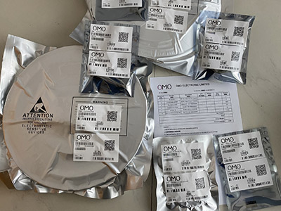
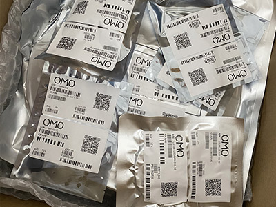
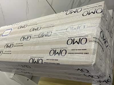
we buy and manage excess electronic components, including excess inventory identified for disposal.
Email us if you have excess stock to sell.

Email: [email protected]
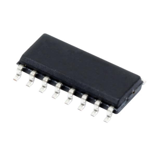
Step1: Vacuum Packaging with PL
Step1:
Vacuum Packaging with PL
Step2: Anti-Static Bag
Step2:
Anti-Static Bag
Step3: Packaging Boxes
Step3:
Packaging Boxes
***as Instruments
CMOS BCD To 7-Segment LCD Decoder/Driver with Strobed-Latch Function 16-SOIC -55 to 125
***an P&S
CMOS BCD To 7-Segment LCD Decoder/Driver with Strobed-Latch Function
***p One Stop Global
Latch/Decoder/Driver Single 4-to-7 16-Pin SOIC T/R
*** Source Electronics
IC BCD-7SEG DECODER/DVR 16SOIC
***i-Key
IC DRVR 7 SEGMENT 1 DIGIT 16SOIC
***ark
Decoder/driver, Bcd To 7 Seg, Soic-16; Logic Family / Base Number:cd4056; Logic Type:bcd To 7 Segment Decoder / Driver; No. Of Outputs:7Outputs; Logic Case Style:soic; No. Of Pins:16Pins; Supply Voltage Min:3V; Supply Voltage Rohs Compliant: Yes
***ment14 APAC
Prices include import duty and tax. DECODER/DRIVER, BCD TO 7 SEG, SOIC-16; Logic Family / Base Number:CD4056; Logic Type:BCD to 7 Segment Decoder / Driver; No. of Outputs:7Outputs; Logic Case Style:SOIC; No. of Pins:16Pins; Supply Voltage Min:3V; Supply Voltage Max:18V; Logic IC Family:CD4000; Logic IC Base Number:4056; Operating Temperature Min:-55°C; Operating Temperature Max:125°C; Product Range:-; Automotive Qualification Standard:-; RoHS Phthalates Compliant:Yes; MSL:MSL 1 - Unlimited; SVHC:No SVHC (27-Jun-2018)
***nell
DECODER/DRIVER, BCD - 7 SEG, SOIC-16; Famiglia Logica / Numero Base:CD4056; Tipo di Logica:Decoder / Driver da BCD a 7 Segmenti; No. di Uscite:7Uscite; Modello Case CI Logico:SOIC; No. di Pin:16Pin; Tensione di Alimentazione Min:3V; Tensione di Alimentazione Max:18V; Famiglia CI Logico:CD4000; Numero Base CI Logico:4056; Temperatura di Esercizio Min:-55°C; Temperatura di Esercizio Max:125°C; Gamma Prodotti:-; Standard di Qualifica Automotive:-; Livello di Sensibilità all'Umidità (MSL):MSL 1 - Non Limitata; Sostanze Estremamente Preoccupanti (SVHC):No SVHC (27-Jun-2018)
***AS USD
CD4055B and CD4056B types are single-digit BCD-to-7-segment decoder/driver circuits that provide level-shifting functions on the chip. This feature permits the BCD input-signal swings (VDD to VSS) to be the same as or different from the 7-segment output-signal swings (VDD to VEE). For example, the BCD input-signal (VDD to VSS) may be as small as 0 to -3 V, whereas the output-display drive-signal swing (VDD to VEE) may be as large as from 0 to -15 V. If VDD to VEE exceeds 15 V, VDD to VSS should be at least 4V (0 to -4V). The 7-segment outputs are controlled by the DISPLAY-FREQUENCY (DF) input which causes the selected segment outputs to be low, high, or a square-wave output (for liquid-crystal displays). When the DF input is low the output segments will be high when selected by the BCD inputs. When the DF input is high, the output segments will be low when selected by the BCD inputs. When a square-wave is present at the DF input, the selected segments will have a square-wave output that is 180° out of phase with the DF input. Those segments which are not selected will have a square-wave output that is in phase with the input. DF square-wave repetition rates for liquid-crystal displays usually range form 30 Hz (well above flicker rate) to 200 Hz (well below the upper limit of the liquid-crystal frequency response). The CD4055B provides a level-shifted high-amplitude DF output which is required for driving the common electrode in liquid-crystal displays. The CD4056B provides a strobed-latch function at the BCD inputs. Decoding of all input combinations on the CD4055B and CD4056B provides displays of 0 to 9 as well as L, P, H, A, -, and a blank position.
***
The CD4054B provides level shifting similar to the CD4055B and CD4056B independently strobed latches, and common DF control on 4 signal lines. The CD4054B is intended to provide drive-signal compatibility with the CD4055B and CD4056B 7-segment decoder types for the decimal point, colon, polarity, and similar display lines. A level-shifted high-amplitude DF output can be obtained from any CD4054B output line by connecting the corresponding input and strobe lines to a low and high level, respectively and applying a square wave to DFIN. The CD4054B may also be utilized for logic-level "up conversion" or "down conversion". For example, input-signal swings (VDD to VSS) for +5 to 0 V can be converted to output-signal swings (VDD to VEE) of +5 to -5 V. The level-shifted function on all three types permits the use of different input- and output-signal swings. The input swings from a low level of VSS to a high level of VDD while the output swings from a low level of VEE to the same high level of VDD. Thus, the input and output swings can be selected independently of each other over a 3-to 18 V range. VSS may be connected to VEE when no level-shift function is required.
***XS
For the CD4054B and CD4056B, data are transferred from input to output by placing a high voltage level at the strobe input. A low voltage at the strobe input latches the data input and the corresponding output segments remain selected (or non-selected) while the strobe is low.
***ASIN
Whenever the level-shifing function is required, the CD4055B can be used by itself to drive a liquid-crystal display (Fig.16 and Fig.20). The CD4056B, however, must be used together with a CD4054B to provide the common DF output (Fig.19). The capability of extending the voltage swing on the negative end (this voltage cannot be extended on the positive end) can be used to advantage in the setup of Fig.18. Fig.17 is common to all three types.
***AS INSRUMENTS
The CD4054B-, CD4055B-, and CD4056B-series types are supplied in 16-lead dual-in-line plastic packages (E suffix), 16-lead small-outline packages (M, M96, MT and NSR suffixes), and 16-lead thin shrink small-outline packages (PW and PWR suffixes). The CD4054B- and CD4056B-series types also are supplied in 16-lead hermetic dual-in-line ceramic packages (F3A suffix).
画像 モデル 説明
CD40193BNSRE4

Mfr.#: CD40193BNSRE4

OMO.#: OMO-CD40193BNSRE4

Counter ICs CMOS Presettable Bin Up/Down Counter
TLV1701AIDBVR

Mfr.#: TLV1701AIDBVR

OMO.#: OMO-TLV1701AIDBVR

Analog Comparators 2.2-V to 36-V 5-SOT-23 -40 to 125
TLV170IDR

Mfr.#: TLV170IDR

OMO.#: OMO-TLV170IDR

Operational Amplifiers - Op Amps 36V microPower R-R Output G Purp Op Amp
SS10P3HM3_A/H

Mfr.#: SS10P3HM3_A/H

OMO.#: OMO-SS10P3HM3-A-H

Schottky Diodes & Rectifiers 10A,30V,SM SKY RECT.
ADR5041AKSZ-REEL7

Mfr.#: ADR5041AKSZ-REEL7

OMO.#: OMO-ADR5041AKSZ-REEL7

Voltage References Prec Micropwr Shunt Mode 2.5 Vout
CD4071BM96

Mfr.#: CD4071BM96

OMO.#: OMO-CD4071BM96

Logic Gates CMOS Quad 2-Input OR
MPXV5100DP

Mfr.#: MPXV5100DP

OMO.#: OMO-MPXV5100DP

Board Mount Pressure Sensors SOP DUAL PORT
UUD1C471MNL1GS

Mfr.#: UUD1C471MNL1GS

OMO.#: OMO-UUD1C471MNL1GS

Aluminum Electrolytic Capacitors - SMD 16volts 470uF
TLV1701AIDBVR

Mfr.#: TLV1701AIDBVR

OMO.#: OMO-TLV1701AIDBVR-TEXAS-INSTRUMENTS

Analog Comparators 2.2-V to 36-V 5-SOT-23 -40 to 125
SA56-51PBWA/A

Mfr.#: SA56-51PBWA/A

OMO.#: OMO-SA56-51PBWA-A-758

LED Displays & Accessories Blue diffused 1 Digit
可用性
ストック:
12
注文中:
1995
数量を入力してください:
CD4056BM96の現在の価格は参考用です。最高の価格をご希望の場合は、お問い合わせまたは直接メールで営業チーム[email protected]までご連絡ください。
参考価格(USD)
単価
小計金額
1
$0.44
$0.44
10
$0.37
$3.68
100
$0.22
$22.40
1000
$0.17
$173.00
2021年から半導体が不足しているため、2021年以前の通常価格以下の価格です。お問い合わせください。
皮切りに
最新の製品
  • CC2540 Bluetooth System-on-Chip
    OMO Electronic' CC2540 is a cost-effective, low-power, true system-on-chip (SoC) for Bluetooth® low energy applications.
  • Compare CD4056BM96
    CD4056BM96 vs CD4056BM96SOP vs CD4056BM96E4
  • LP5907 Linear Regulator
    LP5907 linear regulators have low quiescent current and lead its class in noise performance without the use for a noise bypass capacitor.
  • CC2630/40/50 SimpleLink Wireless MCUs
    The OMO Electronic' CC2630 / CC2640 / CC2650 family of cost-effective, ultra-low power, 2.4 GHz RF devices have very-low active RF and MCU current.
  • MSP-TS430RGZ48C Target Board
    MSP-TS430RGZ48C target boards feature unified FRAM memory, enhanced MSP430 DNA, and integrated analog and digital peripherals.
  • TPA3144D2 Class-D Audio Power Amplifier
    OMO Electronic' TPA3144D2 is an efficient, Class-D audio power amplifier for driving bridged-tied stereo speakers at up to 6 W, 6 Ω, or 8 Ω (per channel).
Top