We guarantee 100% customer satisfaction.
Quality GuaranteesWe provide 90-360 days warranty.
If the items you received were not in perfect quality, we would be responsible for your refund or replacement, but the items must be returned in their original condition.
Our experienced sales team and tech support team back our services to satisfy all our customers.
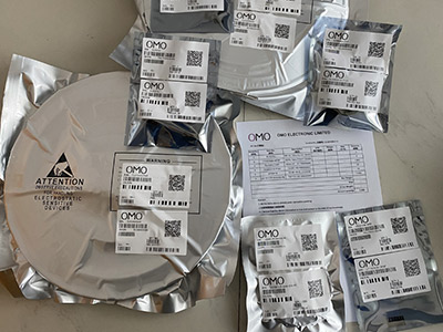
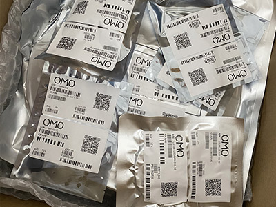
we buy and manage excess electronic components, including excess inventory identified for disposal.
Email us if you have excess stock to sell.
Email: [email protected]
| Part # | Description | Stock | Price |
|---|---|---|---|
| CDC857-3DGGG4 DISTI # CDC857-3DGGG4-ND | IC 3.3V PLL CLK-DRVR 48-TSSOP RoHS: Compliant Min Qty: 80 Container: Tube | Limited Supply - Call | |
| CDC857-3DGGG4 DISTI # 595-CDC857-3DGGG4 | Phase Locked Loops - PLL Phase-Lock Loop Clock Drivers RoHS: Compliant | 0 |
| Image | Part # | Description |
|---|---|---|

|
Mfr.#: CDC857-2DGGRG4 OMO.#: OMO-CDC857-2DGGRG4 |
Clock Drivers & Distribution Phase-Lock Loop Clock Drivers |
|
|
Mfr.#: CDC857-2DGG OMO.#: OMO-CDC857-2DGG |
Clock Drivers & Distribution Phase-Lock Loop Clock Drivers |
|
Mfr.#: CDC857 OMO.#: OMO-CDC857-1190 |
New and Original |
|
|
Mfr.#: CDC857-2 OMO.#: OMO-CDC857-2-1190 |
New and Original |

|
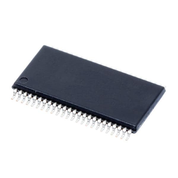
Mfr.#: CDC857-3DGG |
IC 3.3V PLL CLK-DRVR 48-TSSOP |
|
|
Mfr.#: CDC857-3DGGR OMO.#: OMO-CDC857-3DGGR-1190 |
PLL Based Clock Driver, 10 True Output(s), 0 Inverted Output(s), PDSO48 |
|
|
Mfr.#: CDC8573DGGR OMO.#: OMO-CDC8573DGGR-1190 |
New and Original |
|
|
Mfr.#: CDC857B OMO.#: OMO-CDC857B-1190 |
New and Original |
|
|
Mfr.#: CDC857-2DGGR |
Clock Drivers & Distribution Phase-Lock Loop Clock Drivers |
|
|
Mfr.#: CDC857-2DGG |
Clock Drivers & Distribution Phase-Lock Loop Clock Drivers |


