The full name of an NMOS transistor is N-channel Metal-Oxide-Semiconductor Field-Effect Transistor (MOSFET).
This name shows its key features:
N-channel means the device conducts current through an N-type channel. Electrons are the main carriers.
Metal-Oxide-Semiconductor describes the physical structure: a metal gate, an oxide insulating layer, and a semiconductor substrate.
Field-Effect means its operation is based on controlling current with an electric field.
This naming method shows both the structure and the principle of the device. Compared with some modern compound semiconductor devices, NMOS keeps a simple and efficient design. This is one important reason why it is widely used in integrated circuits (ICs).
Basic Working Principle
The key principle of NMOS is that the gate voltage (V_GS) controls the channel between the source (S) and the drain (D).
When the gate voltage is zero or lower than the threshold voltage (V_th), the P-type substrate forms two back-to-back PN junctions. No current flows, and the device is off.
When the gate voltage is positive and larger than V_th (V_GS > V_th), the electric field creates negative charges on the surface of the P-type substrate. This forms an N-type conductive channel between the source and the drain. Then, electrons flow from source to drain, and the device is on.
Because of this voltage control, NMOS has very high input impedance. The gate draws almost no current. It needs only very small driving power. Compared with a Bipolar Junction Transistor (BJT), NMOS makes circuit design easier and reduces power use.
Main Features
NMOS transistors have several clear features:
Voltage control: The gate takes almost no current. Input impedance is very high (up to 10^12 Ω). This makes the driving circuit simple.
Unipolar conduction: Only electrons conduct current. There is no minority carrier storage effect. Switching is faster.
Easy manufacturing: NMOS is simpler to produce, small in size, and uses low power.
Modern processors may contain billions of NMOS transistors in nanometer size, working together for complex computing tasks.
Common Types
There are two main types of NMOS transistors:
Enhancement-mode NMOS: The default state is off. A positive gate voltage is needed to create a conductive channel. This makes it useful as a switch in digital circuits.
Depletion-mode NMOS: The default state is on. A negative gate voltage is needed to turn it off. This type is rare and used only in special cases.
Most modern ICs use enhancement-mode NMOS because it has better off-state control and lower static power use.
Structure of NMOS Transistor
Four-Terminal Device
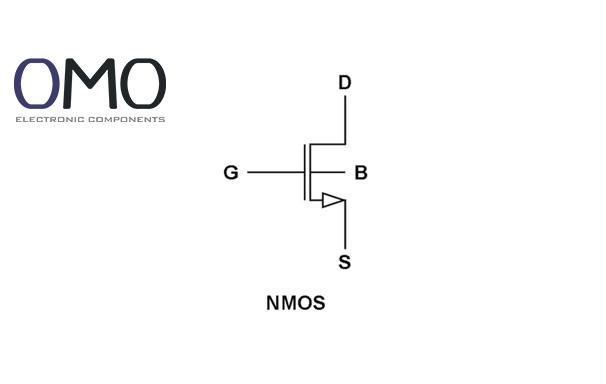
An NMOS transistor has four terminals:
Source (S): starting point of electrons, usually at lower voltage.
Drain (D): end point of electrons, usually at higher voltage.
Gate (G): made of metal or polysilicon, separated from the substrate by an insulator.
Body/Bulk (B): the substrate, usually P-type silicon.
In most circuits, the body is tied to the lowest potential (ground for NMOS) to reduce the body effect. In ICs, all NMOS transistors share the same substrate, so designers must take care of isolation and potential control.
Physical Structure
From bottom to top:
P-type silicon substrate.
Two N+ regions formed by ion implantation → source and drain.
The thickness of the gate oxide is very important. In modern technology, it can be only a few atomic layers. This needs extremely high manufacturing precision.
Working Characteristics of NMOS
Three Operating Regions
NMOS has three regions:
Cutoff region: V_GS < V_th. No channel. Current I_DS ≈ 0. The device is off.
Linear region (Ohmic/Triode): V_GS > V_th and V_DS < (V_GS - V_th). The channel is formed. Current changes linearly with voltage. The device acts like a variable resistor.
Saturation region: V_GS > V_th and V_DS ≥ (V_GS - V_th). The channel is pinched at the drain side. Current becomes stable. This region is used for amplification.
Current-Voltage (I-V) Characteristics
Output characteristic curve: plots I_DS vs. V_DS for different V_GS. It shows the three regions.
Transfer characteristic curve: plots I_DS vs. V_GS (in saturation). Approximate square-law:
I_DS = (μ_n C_ox W / 2L) × (V_GS - V_th)²
where μ_n is electron mobility, C_ox is oxide capacitance, W is channel width, and L is channel length.
Symbols of NMOS
Standard Four-Terminal Symbol
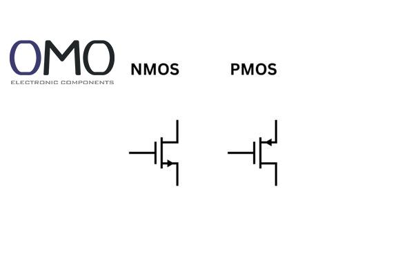
In circuit diagrams, NMOS is shown with four terminals: S, D, G, and B. The arrow points into the channel for NMOS (opposite for PMOS). This helps identify the type quickly.
Simplified Three-Terminal Symbol
In practice, the body terminal is often not drawn, because it is usually tied to ground. The symbol then has only S, D, and G.
Applications and Circuit Design
Use in Digital Circuits
NMOS is very important in digital circuits:
In CMOS inverter, NMOS and PMOS work together to form a power-efficient NOT gate.
NMOS builds the pull-down network, which works with PMOS pull-up network to create logic gates (NAND, NOR, XOR).
In memory:
SRAM cell uses 6 transistors (4 NMOS + 2 PMOS).
DRAM cell uses 1 NMOS + 1 capacitor.
The fast switching and low leakage of NMOS make high-density memory possible.
Use in Analog Circuits
In analog design, NMOS can be used as:
Amplifiers:
Common-source (high voltage gain).
Common-gate.
Common-drain / Source follower (buffer).
Analog switches: to pass or block signals.
Active loads or current mirrors: to provide stable bias currents.
Compared with BJTs, NMOS offers higher input impedance and better linearity in low-voltage designs.
Design Considerations
When designing with NMOS:
Body effect: If source and body voltages differ, V_th changes.
W/L ratio: affects drive strength. Larger W gives higher current but larger area. Smaller L increases speed but causes short-channel effects.
Modern NMOS design uses channel engineering to reduce short-channel problems while keeping small size.
NMOS vs PMOS
Comparison of Features
Feature
NMOS Transistor
PMOS Transistor
Channel type
N-type (electrons)
P-type (holes)
Carrier
Electrons
Holes
Threshold voltage V_th
Positive (+)
Negative (-)
Turn-on condition
V_GS > V_th
V_GS < V_th
Power polarity
Usually + supply
Usually - supply or ground
Symbol arrow
Inward (to channel)
Outward
Carrier mobility
High (~500 cm²/V·s)
Lower (~200 cm²/V·s)
On-resistance R_on
Lower
Higher
NMOS has higher electron mobility (about 2.5× that of holes). This means higher current and faster switching. That is why NMOS is often used in speed-critical paths.
Complementary Structure and CMOS
CMOS (Complementary MOS) combines NMOS and PMOS in one chip.
Main advantage: very low static power. In steady state, one transistor is always off, so almost no current flows.
CMOS also has good noise immunity and power scaling.
Modern CMOS has reached 3 nm technology, with over 10 billion transistors on a single chip. This success is possible because of both NMOS and PMOS.
Frequently Asked Questions
What is the difference between NMOS and PMOS transistors?
NMOS transistors employ electrons as charge carriers and are activated by a positive gate-to-source voltage. Conversely, PMOS transistors use holes and require a negative gate-to-source voltage to turn on.
What's the difference between CMOS and NMOS?
Leveraging complementary pairs of NMOS and PMOS transistors, CMOS technology achieves low power consumption and high noise immunity. This differs from NMOS architecture, which relies solely on NMOS transistors.
Why is NMOS preferred over PMOS?
Owing to greater electron mobility, NMOS transistors offer faster switching and lower on-resistance than PMOS, advantages that are critical for high-speed, efficiency-driven applications.
What are the disadvantages of NMOS?
Compared to CMOS technology, NMOS transistors exhibit higher power consumption and slower speeds in complex circuit designs. This is primarily because their structure lacks a complementary PMOS pull-up network, resulting in a continuous static current when in the 'on' state.